Nanotechnology is driving some of today’s most exciting engineering breakthroughs, and for those on the forefront of nanotechnology research, the clean room is the ultimate playground.
Nanotechnology simply refers to engineering on the nanoscale, with one nanometer being over a thousand times smaller than the width of a human hair. While working on the nanoscale enables researchers to interact with the world in an amazing way, it likewise means that a single human hair can possibly damage thousands of nanoscale devices.
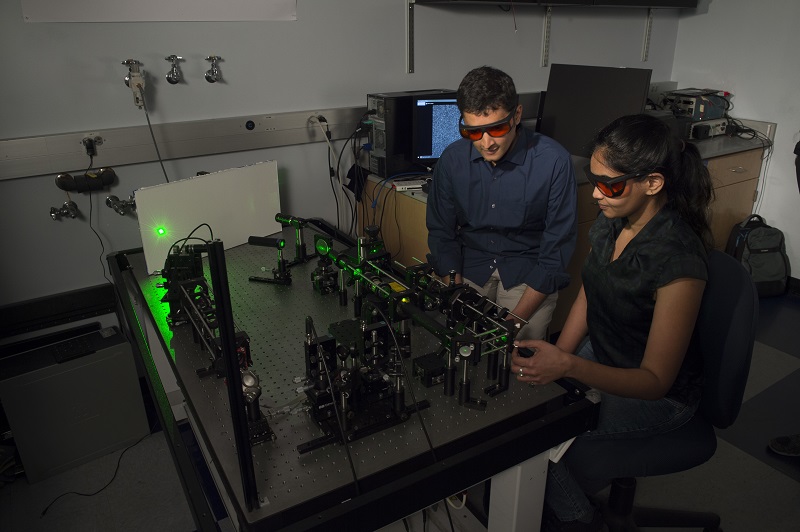
As such, nanotechnology research is carried out in clean rooms that provide the opportunity to play with nanoscale engineering without having to worry about contamination from particles. Researchers gowned in particle-blocking suits, yellow rooms blocking high-energy light, and tools operating under vacuum, all come together to support this important field of research.

Clean Rooms Are Transforming Nanotechnology Research
Historically, researcher’s venture into the world of nanotechnology has been facilitated by the desire to shrink transistors. Smaller transistors enable more efficient and higher performing complimentary semiconductor-metal-oxide (CMOS) chips — the workhorse behind today’s data infrastructure. Such physical scaling, captured through Moore’s Law, has allowed us to decrease the scale that engineers can play on by over three orders-of-magnitude, from micrometers to nanometers.
Presently, the world’s leading semiconductor foundries are working on devices that are only a few nanometers long. While clean room research refers to much more than transistor scaling, most of the tools that allow researchers to work and see on the nanoscale were developed under the pursuit of CMOS scaling. Today, cleanrooms are home to engineers, physics, chemists, biologists, and more.
SMU's State-of-the-Art Clean Room
SMU houses one of the largest academic cleanrooms and is home to diverse nanotechnology research. The SMU clean room is distributed across class 10 and class 1000 bays with tools for growing new materials, characterizing these materials, and fabricating these materials into nanoelectronic devices like transistors, lasers, and sensors, to name a few. The facility supports the growth of compound semiconductors for optoelectronics, silicon and oxides for micro-electro-mechanical-systems (MEMS), and two-dimensional (2D) materials for fundamental research in device physics. The photolithography bay includes resist coating, mask aligners, and development hoods.
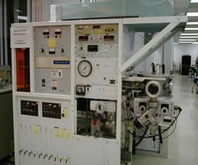
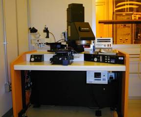
The facility provides numerous etching tools, such as plasma etching, and tools for the deposition of metals and oxides, such as electron-beam evaporation, plasma-enhanced chemical vapor deposition, and sputtering. Regarding characterization, the facility is home to numerous microscopes, ellipsometers, and profilometers. Cryogenic probe stations are also available in shared lab space to electrically test devices at low-temperature and under vacuum.
Explore SMU's Current Research Projects
There are a variety of research groups that are actively involved in clean room research at SMU. This includes groups led by Professor J.C. Chiao, Professor Bruce Gnade, Professor Gary Evans, and Professor Duncan MacFarlane. In particular, my research group is exploring 2D materials, like graphene, that are only a single atom thick. These 2D materials can be thought of as the ultimate limit of nanoscale engineering; a single layer of atoms is only a fraction of a nanometer thick. Working with 2D materials allow researchers to play with the fundamental physics of how charge and heat flows through a material. The hope is that discoveries at the atomic-level can lead to the development of wildly new nanoelectronics.
Current 2D material research at SMU is focused on creating flexible circuits, enabling integrated circuits to be built in 3D, and developing new biological sensors that support data-driven healthcare. Clean room research at SMU is not limited to nanoelectronics and also involves explorations of biological and quantum systems.
For more information on SMU's Ph.D. in Engineering degrees, opportunities to conduct clean room-based research, and how to further advance your graduate studies, download "The Degree that is Propelling Society Forward: A Complete Guide to Earning Your Ph.D. in Electrical and Computer Engineering."
Check out our new digital resource to explore more topics of Electrical and Computer Engineering research happening at SMU!